
Project C08 - Components for Mobile Broadband Passive Imaging
Systems
Principal Investigators: Prof. Dr. Ullrich Pfeiffer; Dr. Sascha Weyers
Achieved Results in the 1st Phase
To address these challenging research questions, the overall frequency band was divided into two subbands (below/above fmax) during the 1st phase of C08.
Radiometry with preamplification (below fmax)
Below fmax where LNAs can provide sufficient gain to boost the receiver performance, a differential five-stage cascode based silicon-integrated high gain, low noise amplifier was developed in an advanced BiCMOS technology from IHP with of 500/700 GHz. The center frequency was moved above 200 GHz to increase the operation bandwidth and profit from the increasing black body power, which grows with frequency and thus counteracts the expected higher Noise Figures in this frequency range.
Radiometry without preamplification (above fmax)
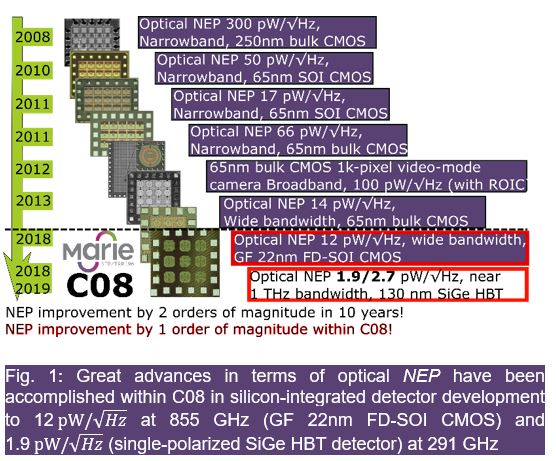
To address the second research question both, sensitivity and even more importantly, bandwidth enhancement strategies, were applied for silicon-integrated antenna-coupled direct detectors in an advanced 130 nm SiGe HBT technology from IHP with 350/550 GHz as well as in a 22 nm FD-SOI CMOS technology from Globalfoundries. Based on an extensive global optimization of the antenna driving impedance and the detector/antenna co-design technique, detector responsivity and NEP were optimized across the operational bandwidth and the transistor biasing point, resulting in direct detectors with state-of-the-art measured optical NEPs between 200 GHz and 1 THz. Within C08, peak values of 12 at 855 GHz (in GF 22nm FD-SOI CMOS) [A], 2.7 at 430 GHz (Dual-polarized SiGe HBT detector) [B], [C] and up to 1.9 (single-polarized SiGe HBT detector) at 290 GHz have been reached [D]. Due to the near one THz fractional bandwidth of each detector, these outperform the previous state-of-the-art optical NEP of silicon-integrated direct detectors in the full bandwidth. Fig. 1 shows the advances in terms of optical NEP achieved at the IHCT Lab in recent years. The world-lowest optical NEP of 14 pW/√Hz at 724 GHz for a room temperature operated THz MOSFET detector in 65 nm CMOS prior to MARIE [E] has been improved by nearly one order of magnitude, outperforming the initial objective during the 1st phase of C08 (7 by more than a factor of two.
Passive system integration
The integration of circuit building blocks, as previously described, together with color filter antennas results in a very challenging multi-antenna system design, where the bandwidth and sensitivity through additional antenna-LNA and LNA-detector matching circuits are minimized. The system consists of a dual-polarized broadband 100 Ohm differential antenna, that was optimized for backside radiation through the silicon die with an external packaged hyper-hemispherical lens resulting in 80 percent simulated radiation efficiency between 180 GHz and 400 GHz. The first antenna path is connected to the proposed 5-stage LNA coupled direct detector. The second path is directly connected to a direct detector. To address the means of color filtering, three narrowband patch-antenna structures for the frequency bands around 400 GHz, 600 GHz, and 800 GHz (60 % efficiency, each) were placed in 200 µm distance, to enable frequency-selectivity. These patches were co-designed and, to reduce the bandwidth, connected by /4 lines with SiGe HBT direct detectors
Camera resolution limits
Within the long-term perspective of C08, joint phase-center frequency filtering antennas, implemented in a passive camera system, will divide the entire RF bandwidth into subbands for the purpose of spectral material analysis. As the resolution for each subband depends on the size of the external silicon lens and the wavelength, an optimum pixel pitch can only be provided at a single frequency in one particular band, whereas the higher frequency band will be under-sampled and the lower over-sampled. This trade-off was investigated, analyzing angular resolution limitations of geometrically separated pixels in lens-integrated THz cameras [F]. An approach that was researched to overcome this resolution limits, is the so-called geometrical multi-frame super-resolution imaging [G].
Preliminary work on microbolometers
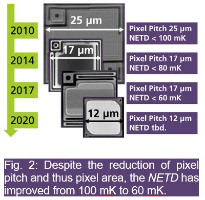
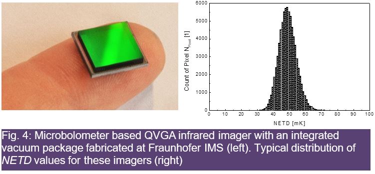
Due to the low sensitivity of electronic circuits above 2 THz, the 2nd phase of C08 addresses the hetero-integration of electronic receivers and absorptive bolometers. Here, preliminary research was done by the Fraunhofer IMS which is the only manufacturer of uncooled microbolometers in Germany. This research focused on passive signal detection in the IR frequency range of 20 to 43 THz (l » 7 µm to 15 µm). Fully integrated imagers, including digital readout and chip-scale vacuum package, have been realized [I]. All components have been developed and are fabricated at the Fraunhofer IMS CMOS and microsystem technology clean rooms. During the microbolometer development process, the pixel pitch is continuously reduced from 25 µm in the first generation towards 17 µm in the following two generations. Currently under development is a microbolometer technology for pixel pitches of 12 µm and below. All of these generations of microbolometers are shown in Fig. 2. This new technology makes use of coreless nanowires providing electrical conductivity, mechanical stability and thermal isolation at the same time [J]. It combines all three key functions required to connect a microbolometer to a readout circuit in one structure. Typically, the thermal isolation is realized in the same plane as the sensing area. Therefore, thermal isolation and sensor are competing for the available area. Decreasing pixel pitch results in a significant loss of sensing area. By moving the thermal isolation out of the sensor plane into the perpendicular electrical and mechanical connection the sensor area can be maximized and the thermal isolation can be made independent from the pixel pitch. This results in a maximized sensitivity and a high degree of freedom in the microbolometer design.
Besides microbolometers, coreless nanowires have been used at Fraunhofer IMS for various developments and applications. Their ability to provide electrical contact and thermal isolation at the same time led to their use in devices like thermopiles and pellistors. Coreless nanowires have also been used in applications where only mechanical and electrical properties are important. One of these applications are electrodes to contact biological cells.
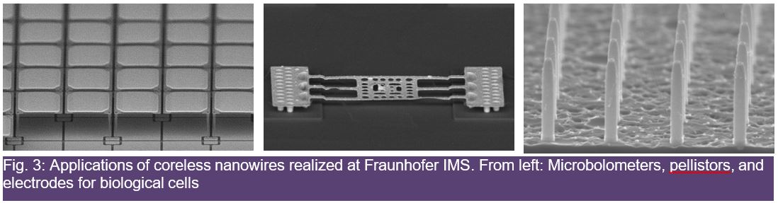
Besides microbolometers, coreless nanowires have been used at Fraunhofer IMS for various developments and applications. Their ability to provide electrical contact and thermal isolation at the same time led to their use in devices like thermopiles and pellistors. Coreless nanowires have also been used in applications where only mechanical and electrical properties are important. One of these applications are electrodes to contact biological cells. Furthermore, they have been realized for stimulation as well as sensing in the cells. Currently under development are coreless nanowires that can also be used to inject substances into cells. Materials and shapes of coreless nanowires are chosen depending on the application, using common base technology for their fabrication. Some of the realized structures are shown in Fig. 3.
References
[1] M. Kowalski and M. Kastek, "Comparative Studies of Passive Imaging in Terahertz and Mid-Wavelength Infrared Ranges for Object Detection", IEEE Transactions on Information Forensics and Security, Sept. 2016.
[2] J- May and G. Rebeiz, "Design and characterization of W-band SiGe RFICs for passive millimeter-wave imaging," IEEE Transactions on Microwave Theory and Techniques, May 2010.
[3] J. Lynch et al., "Passive Millimeter-Wave Imaging Module With Preamplified Zero-Bias Detection," IEEE Transactions on Microwave Theory and Techniques, July 2008.
[4] F. Caster II et al., "Design and Analysis of a W-band 9-Element Imaging Array Receiver Using Spatial-Overlapping Super-Pixels in Silicon," IEEE Journal of Solid-State Circuits, April 2014.
[5] A. Tang, Y. Kim, and Q. Gu, "A 0.43K NETD 100GHz Dicke-Free Radiometer with 100% Time Efficiency n 65nm CMOS," IEEE International Solid-State Circuits Conference, January 2016.
[6] H. Rücker, B. Heinemann, “High-performance SiGe HBTs for next generation BiCMOS technology”, Semiconductor Science and Technology, October 2018.
[7] A. Tang, Y. Kim, and Q. Gu, "Broadband terahertz imaging with highly sensitive silicon CMOS detectors", Optics Express, April 2011
[8] Boppel, Lisauskas et. al., “CMOS Integrated Antenna-Coupled Field-Effect Transistors for the Detection of Radiation From 0.2 to 4.3 THz”, IEEE Transactions on Microwave Theory and Techniques, Dec 2012.
[9] M. Schröter et al., "SiGe HBT Technology: Future Trends and TCAD-Based Roadmap", Proceedings of the IEEE, June 2017
[10] N. Oda, "Technology trend in real-time, uncooled image sensors for sub-THz and THz wave detection", Proceedings of SPIE, Micro- and Nanotechnology Sensors, May 2016
[11] F. Simoens, J. Meilhan, J., and J-A. Nicholas, “Terahertz Real-Time Imaging Uncooled Arrays Based on Antenna-Coupled Bolometers or FET Developed at CEA-Leti”, Journal of Infrared, Millimeter, and Terahertz Waves, August 2015
[12] D. Dufour et al., “Review of terahertz technology development at INO”, Journal of Infrared, Millimeter, and Terahertz Waves, July 2015
Project-related publications by participating researchers
[A] R. Jain, R. Zatta, J. Grzyb, D. Harame, U. R. Pfeiffer, “A Terahertz Direct Detector in 22nm FD-SOI CMOS”, 13th European Microwave Integrated Circuits Conference, September 2018
[B] J. Grzyb, M. Andree, R. Jain, B. Heinemann and U. R. Pfeiffer, "A Lens-Coupled On-Chip Antenna for Dual-Polarization SiGe HBT THz Direct Detector", IEEE Antennas and Wireless Propagation Letters, November 2019
[C] M. Andree, J. Grzyb, R. Jain, B. Heinemann and U. R. Pfeiffer, "A Broadband Dual-Polarized Terahertz Direct Detector in a 0.13-μm SiGe HBT Technology", IEEE MTT-S International Microwave Symposium, June 2019
[D] M. Andree, J. Grzyb, R. Jain, B. Heinemann and U. R. Pfeiffer, "A Broadband Antenna-Coupled Terahertz Direct Detector in a 0.13-μm SiGe HBT Technology", 14th European Microwave Integrated Circuits Conference, October 2019
[E] P. Hillger, J. Grzyb, R. Jain and U. R. Pfeiffer, "Terahertz Imaging and Sensing Applications With Silicon-Based Technologies", IEEE Transactions on Terahertz Science and Technology, January 2019 – Most popular journal since its appearance in the Transactions on Terahertz Science
[F] R. Zatta, R. Jain, J. Grzyb and U. R. Pfeiffer, "Resolution Limits in Lens-Integrated CMOS THz Cameras Employing Super-Resolution Imaging", 44th International Conference on Infrared, Millimeter, and Terahertz Waves, September 2019
[G] R. Zatta, V. S. Jagtap, J. Grzyb and U. R. Pfeiffer, “CMOS Terahertz Camera Used as Compact Antenna Test Range”, Third International Workshop on Mobile Terahertz Systems, July 2020
[H] P. Hillger, M. van Delden, U. S. Miriya Thanthrige, A. Mostafa Ahmed, J. Wittemeier, K. Arzi, M. Andree, B. Sievert, W. Prost, A. Rennings, D. Erni, T. Much, N. Weimann, A. Sezgin, N. Pohl, U. R. Pfeiffer, “Toward Mobile Integrated Electronic Systems at THz Frequencies”, Journal of Infrared, Millimeter, and Terahertz Waves, June 2020 – MARIE journal publication authored by the IHCT Lab
[I] D. Weiler, F. Hochschulz, C. Busch, M. Stein, M. D. Michel, A. Kuhl, R. Lerch, M. Petermann, T. Geruschke, S. Blaeser, S. Weyers, H. Vogt, “Digital uncooled IRFPAs based on microbolometers with 17 μm and 12 μm pixel pitch”, Proceedings of SPIE, October 2018
[J] K.-M. Muckensturm, D. Weiler, F. Hochschulz, C. Busch, T. Geruschke, S. Wall, J. Heß, R. Lerch, D. Würfel, H. Vogt, “Uncooled microbolometer arrays with a pixel size of 12μm based on a novel thermally isolating structure”, Technisches Messen, March 2017