
Project C01 - UWB Phase-Locked Loops with Highest Phase Stability
Principal Investigator: Prof. Dr.-Ing. Thomas Musch, RUB
Achieved Results in the 1st Phase
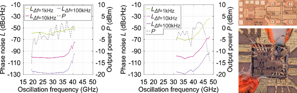
One highlight of the achievements within C01 is the novel YTO [4, 6] with several methods and results. The main idea is to directly mount the Yttrium-Iron-Garnet (YIG) sphere over a Monolithic Microwave Integrated Circuit (MMIC), including the amplifier, and use crossed chip-to-chip bond wires to couple the YIG sphere, as depicted in Fig. 1. This enables realizing a transmission-type YTO at high oscillation frequencies. A transmission-type YTO is favorable, as it prohibits disturbing walker modes, which can occur in a reflection type YTO. To obtain an equivalent circuit of the YIG sphere for the design and circuit simulations of the YTO, a corresponding model of the YIG sphere was elaborated. It is described in detail in [4] and has been proofed to be very accurate. Hence, a method for optimized design and investigations of YTOs is achieved. The YTOs realized in C01 achieve two outstanding results. On the one hand, the YTOs can work up to 48 GHz, which is the highest reported oscillation frequency of YTOs to date. On the other hand, the YTOs achieve the lowest phase noise with respect to the carrier frequency reported so far. The measured phase noise and output power as a function of the oscillation frequency for two realized YTOs is depicted in Fig. 1.
Fig. 1: Measured phase noise for different offset frequencies Δf and output power of two realizations of the novel YTO (left, middle) and a photograph of the YTO chip and mounting of the YIG sphere (right).
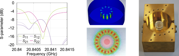
The Sapphire Loaded Cavity Resonator (SLCR) is designed to operate at a high mode (WGE10,0,0) to minimize the evanescent field outside the sapphire and thus increase the quality factor. As there are multiple resonances around the desired mode, a mechanically tunable Dielectric Resonator (DiR) in fundamental mode is utilized as a filter. The realized SLCR exhibits a resonance with a loaded quality factor of approx. 50,000 at 20.8 GHz, which can be calculated from the measured scattering parameters shown in Fig. 2 The corresponding realized dielectric resonator offers a quality factor between 1,050 and 3,200, while it is tunable over approx. 250 MHz. The amplifier is implemented in an MMIC and offers a broadband amplification of 15 dB with an output-referred 1-dB compression point of 1 dBm, while the noise figure is lower than 4 dB with a flicker noise corner of 8 kHz. Applying Leeson’s equation, the resulting phase noise can be estimated to be in the range of ‑120 dBc/Hz and -146 dBc/Hz at an offset frequency of 1 kHz and 10 kHz, respectively.
Fig. 2: Measured scattering parameters (left) and simulated magnetic field (middle) of the SLCR’s WGE10,0,0 mode as well as a photograph of the realized SLCR (right).
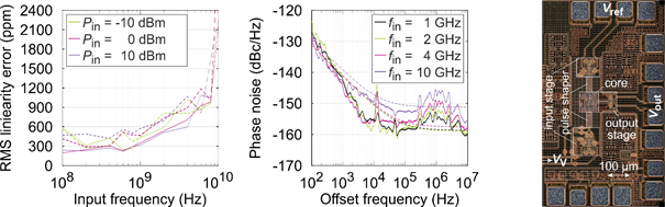
Concerning the frequency divider, different concepts, like a 2/3-divider-cascade [1], dual-modulus synchronous and asynchronous counters, have been investigated. Although the 2/3-divider chain offers a low possible division factor down to two and easy scalability, this is not required in C01, as the swing of the delta-sigma modulation requires higher division factors. In terms of operating speed, and especially phase noise [2], the dual-modulus concept utilizing a prescaler and two synchronous counters is the most promising approach. For the same purpose, the gates were realized in a merged emitter-coupled logic, i.e., logic functions were consequently merged together and into flip flops by stacking differential amplifiers. Moreover, inductive peaking by means of differential spiral inductors as well as transmission lines were applied and optimized to enhance the bandwidth. Doing so, we realized an 8-bit frequency divider operating up to 117 GHz, as depicted in Fig. 3. This is the fastest fully programmable frequency divider reported so far. For this one, a phase noise measurement was not possible yet. With another related version working up to 94 GHz, a low additive phase noise due to the applied synchronization was measured. It exhibits a noise floor of -150 dBc/Hz and a flicker-noise corner of 13 kHz at an output frequency of 1 GHz, as shown in Fig. 3.
Fig. 3: Measured (solid) and simulated (dashed) additive phase phase noise of the 94 GHz frequency divider, as well as measured sensitivity (middle) and photograph of the 117 GHz frequency divider (right).
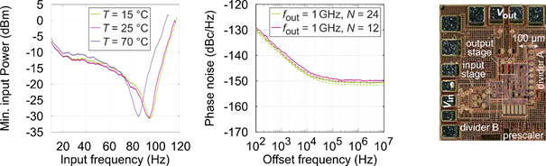
The requirements for the PFD are high operating speed, high linearity, as well as low additive phase noise. Concerning this, we investigated different concepts for the PFD by simulations. The most promising approach is the XOR-based architecture [6]. In phase detection mode, i.e., a phase difference between 0 and 2π, only two flip-flops acting as divide-by-two stages and an XOR gate as PD are active. On the one hand, the additive phase noise is low due to the few gates. On the other hand, the XOR generates a pulse width modulated signal with a 50% duty cycle at a phase difference of π, which is the locking point of the PLL. As only the pulse width will be increased or decreased with the phase difference, the linearity is very high. The realized PFD operates up to 18 GHz and offers an RMS linearity error below 500 ppm for frequencies up to 4 GHz. The measured additive phase noise exhibits a floor of -155 dBc/Hz and a flicker noise corner of 20 kHz at an input frequency of 1 GHz. The measurements of the RMS linearity error and the additive phase noise are depicted in Fig. 4.
Fig. 4: Measured (solid) and simulated (dashed) linearity error (left), additive phase noise (middle), and photograph (right) of the realized PFD.
For the modulation of the frequency and thus the generation of the chirp, the proposed binary DDS concept was investigated. This utilizes a frequency divider with binary output pulses at the frequency fref. By using a fixed input frequency and appropriate modulating of the division factor N ∈ ℕ, it generates a chirp at the output. In C01, the binary DDS is intended to be utilized in the reference path of the PLL. In contrast to the classical modulation of the division factor in the PLL’s feedback path, the calculation of the ideal fractional division factor F ∈ ℚ as a function of cycles k, in this case, is not linear and recursive according to with the chirp bandwidth at the binary DDS’ output BWchirp, the chirp duration Tchirp, and the binary DDS’ input frequency f0. The modulated, integer division factor N is generated by feeding F to a delta-sigma modulation. This concept was proofed by a realization, based on calculating N by a computer and storing it into a discrete Random-Access Memory (RAM). However, due to timing issues, the chirps could only be generated in the frequency bands 50 MHz ≤ fref ≤ 90 MHz, 120 MHz ≤ fref ≤ 175 MHz, and 180 MHz ≤ fref ≤ 220 MHz. A concept to overcome this disadvantage is proposed in WP1 of the 2nd phase. As the chirp is pulsed and sigma-delta modulated, a measurement of the linearity with the available equipment at this point was not feasible.
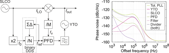
The desired PLL concept [3] is depicted in Fig. 5 and utilizes a YTO and SLCO due to their aforementioned advantages. The novel structure is based on an offset PLL concept, where the SLCO directly acts as a Local Oscillator (LO) for the down-conversion. By generating the frequency chirp using a binary DDS in the reference path, the frequency division factor in the feedback path can be reduced. These measures greatly contribute to a minimized phase noise at the output, while maintaining a high bandwidth and chirp linearity. Due to the novelty, investigations and implementations of PLL simulators are required. The different simulators are capable of simulating the phase noise and transient response, based on the macroscopic parameters of the building blocks including the delta-sigma based chirp generation. Additionally, a full transient simulator including the inner structure of the building blocks was implemented. Based on the components’ measurement results above, we designed and simulated the entire PLL with an output frequency range of 22.5 GHz ≤ fout ≤ 37.5 GHz, corresponding to a relative bandwidth of 50%. The resulting division factors are M = 8 and 19 ≤ N ≤ 197, where the chirp is generated by modulating N. The resulting phase noise contributions and total phase noise are depicted in Fig. 5 for an output frequency of fout = 30 GHz. This corresponds to an integrated jitter of τ = 7.5 fs.
Fig. 5: Block diagram of desired PLL structure (left) and simulated phase noise of the system at an output frequency fout = 30 GHz (right) based on the measured phase noise contributions of the single components.
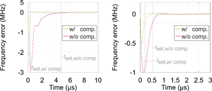
The feasible small loop bandwidth is favorable for the phase noise, but the settling time of the PLL will be comparatively long. As this would decrease the effective usable measurement time and thus bandwidth, a compensation method was investigated. Therefore, a pre-distortion of the divided reference frequency was investigated. The elaborated novel method [5] is based on a state-space model and feed-forward control. This was verified by applying it to two other, fully working PLLs [6], which were investigated and characterized at the Institute of Electronic Circuits. As depicted in Fig. 6, the settling time could be reduced from 4.7 μs to 306 ns and from 500 ns to 228 ns, respectively. However, the minimal measurable settling time was limited by the measurement equipment. In simulations, the method allows for even further reduction.
Fig. 6: Measured (solid) and simulated (dashed) frequency error at the output of the PLLs [I] (left) and [E] (right) with and without the investigated compensation method to reduce the settling time.
References
[1] A. Ergintav, F. Herzel, D. Kissinger, et al., “A 70 GHz static dual-modulus frequency divider in SiGe BiCMOS technology,” in European Microwave Integrated Circuits Conf., Paris, Sep. 2015
[2] S. Levantino, L. Roman, S. Pellerano, C. Samori, and A. L. Lacaita, “Phase noise in digital frequency dividers,” IEEE Journal of Solid-State Circuits, May 2004
Selected Project-related publications
For all project-related publications please click here and scroll to the C01 section.
[3] P. Hillger, M. van Delden, T. Musch et al., “Toward Mobile Integrated Electronic Systems at THz Frequencies,” J Infrared Milli Terahz Waves (2020), DOI: 10.1007/s10762-020-00699-x
[4] M. van Delden, N. Pohl, K. Aufinger, C. Baer, T. Musch, “A Low-Noise Transmission-Type Yttrium Iron Garnet Tuned Oscillator Based on a SiGe MMIC and Bond-Coupling Operating up to 48 GHz,” IEEE Transactions on Microwave Theory and Techniques, Oct. 2019
[5] L. Polzin, M. van Delden, T. Musch, “A Feed-Forward Control Based Method to Reduce the Settling Time of Phase-Locked Loops for Frequency Ramp Synthesis”, in German Microwave Conf., Stuttgart, Mar. 2019
[6] M. van Delden, N. Pohl, K. Aufinger, T. Musch, “A 32-48 GHz Differential YIG Oscillator with Low Phase Noise Based On a SiGe MMIC”, in IEEE Radio and Wireless Symposium, Orlando, Jan. 2019
[7] M. van Delden, N. Pohl, T. Musch, “An Ultra-Wideband, Fast Frequency Ramp Synthesizer at 60 GHz with Low Noise Using a New Loop Gain Compensation Technique,” IEEE Transactions on Microwave Theory and Techniques, Sep. 2018.